IBM has announced a transistor design operating below the one-nanometre threshold — a development that analysts and policymakers say could fundamentally alter the global semiconductor landscape, with direct implications for Britain's industrial strategy and its ambitions to become a serious player in advanced chip manufacturing.
The announcement, which follows years of incremental gains in silicon miniaturisation, represents a potential inflection point in computing performance and energy efficiency. For the United Kingdom, a country that has spent considerable political capital on repositioning itself as a technology superpower post-Brexit, the timing is both an opportunity and a warning.
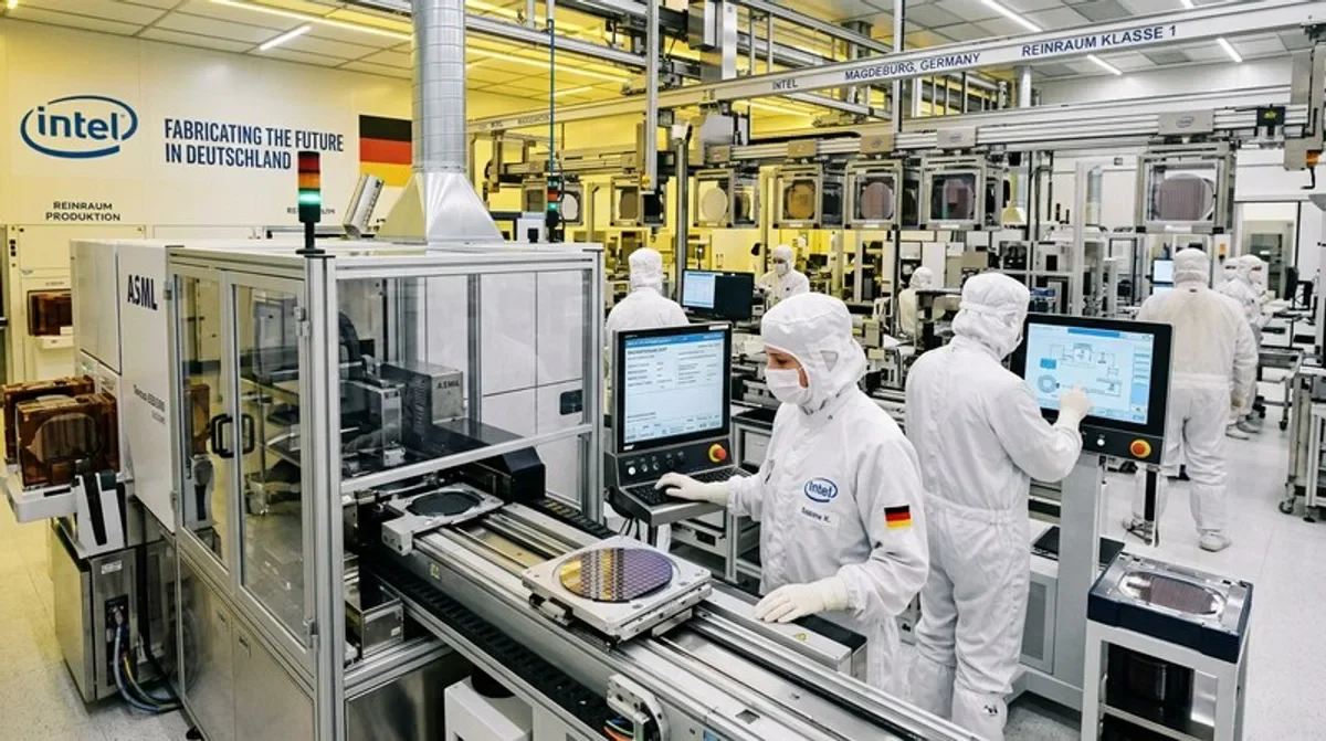
Key Data: A nanometre is one billionth of a metre. Current leading-edge chips from TSMC and Samsung are manufactured at 3nm or 2nm process nodes. IBM's sub-1nm transistor research, conducted in partnership with Samsung and others, suggests the next generation of chips could deliver up to 85% power reduction compared to existing 7nm designs, according to IBM Research. The global semiconductor market is projected to exceed $1 trillion by the end of this decade (Source: Gartner). The UK currently holds less than 1% of global chip fabrication capacity (Source: UK Semiconductor Advisory Panel).
What IBM's Breakthrough Actually Means
To understand the significance of IBM's announcement, it helps to grasp what transistor scaling involves. A transistor is the fundamental switching unit inside a processor — billions of them toggle between on and off states to perform calculations. The smaller each transistor, the more can be packed onto a single chip, and the more efficiently they operate. For decades, the industry followed Moore's Law, the observation by Intel co-founder Gordon Moore that transistor counts double roughly every two years.
The Physics Problem
At sub-nanometre scales, the laws of classical physics begin to break down. Electrons no longer behave predictably — they can tunnel through barriers they should theoretically be blocked by, causing errors and heat. IBM's research, detailed in findings covered by MIT Technology Review, uses a novel gate-all-around nanosheet architecture that wraps the transistor's control electrode around the channel on all sides, giving engineers far greater control over electron flow at atomic scales.
This is not a chip available for purchase. It is a research milestone demonstrating that sub-1nm transistors are physically achievable, a distinction that matters enormously when separating genuine scientific progress from marketing claims that have plagued the industry. (Source: MIT Technology Review)
Energy Efficiency as the New Performance Metric
Raw speed is no longer the primary competitive axis in semiconductor design. With data centres currently consuming an estimated 1–2% of global electricity — a figure rising sharply as artificial intelligence workloads expand — energy efficiency per computation has become the dominant engineering priority. IBM's sub-1nm design reportedly achieves transistor density and power characteristics that, if replicated at manufacturing scale, could dramatically reduce the energy footprint of AI inference and training operations. (Source: Wired)
Britain's Semiconductor Position: Ambition Versus Reality
The United Kingdom's semiconductor strategy has been a source of ongoing tension between stated ambition and measurable capacity. Britain is home to strong design expertise — ARM Holdings, headquartered in Cambridge, licenses chip architectures used in virtually every smartphone on the planet — but the country lacks the advanced fabrication facilities, known as fabs, that turn designs into physical silicon at scale.
The government's semiconductor strategy, published previously and updated with additional investment commitments, explicitly acknowledges this gap. It prioritises compound semiconductors, chip design, and research infrastructure rather than attempting to compete directly with TSMC's gigafabs in Taiwan or Intel's planned European expansion.
Newport Wafer Fab and the Geopolitical Dimension
The contested acquisition of Newport Wafer Fab in Wales — eventually subject to government intervention on national security grounds — illustrated how acutely Whitehall has come to regard semiconductor supply chains as a strategic vulnerability. The facility, which manufactures compound semiconductors used in defence, telecoms, and automotive applications, became a proxy for wider debates about foreign ownership of critical infrastructure. (Source: Reuters)
IBM's breakthrough adds fresh urgency to those debates. If sub-1nm fabrication becomes the new standard within the next decade, countries without sovereign manufacturing capability at advanced nodes risk permanent technological dependency — not just commercially, but in areas of national security where chip supply cannot be outsourced.
UK Research Infrastructure: Points of Genuine Strength
Britain's position is not uniformly weak. Its university research base, particularly in materials science, quantum physics, and electrical engineering, is internationally competitive. The country has invested in national facilities including the Henry Royce Institute and the National Quantum Computing Centre, and British universities have attracted significant partnership interest from major technology companies.
Earlier this year, King's College London secured access to Google's quantum chip hardware in a research partnership that signals ongoing American confidence in British academic institutions as serious collaborators in frontier technology. Quantum computing and advanced classical semiconductor research are increasingly adjacent fields, particularly as both explore post-silicon materials and quantum effects at nanoscale.
The Design-Fabrication Gap
Britain's chip design ecosystem has also demonstrated it can produce globally significant work beyond ARM. Bristol-based Graphcore built an entirely new class of AI processor — the Intelligence Processing Unit — that attracted billions in investment and drew comparisons to ARM's own disruptive origins. Such examples demonstrate that British engineers are capable of architectural innovation even when manufacturing must be outsourced abroad.
The critical policy question is whether design excellence alone is sufficient in a world where fabrication nations — Taiwan, South Korea, the United States, and increasingly Japan and the EU — are treating chip manufacturing as a matter of economic sovereignty. IDC analysts have warned that the concentration of leading-edge fabrication in fewer than five facilities globally represents a systemic supply chain risk that design-only strategies cannot fully mitigate. (Source: IDC)
Industrial Strategy Implications
IBM's announcement arrives as the UK government is under pressure to sharpen its industrial strategy around tangible technology investments rather than broad frameworks. The semiconductor sector has repeatedly been cited by business groups and academic bodies as an area where public investment catalyses private commitment — a dynamic visible in the United States CHIPS and Science Act and the EU Chips Act, both of which allocated tens of billions in subsidies to attract or retain advanced manufacturing.
Britain's equivalent commitments have been substantially smaller in absolute terms, though officials argue that targeted investment in areas of comparative advantage — compound semiconductors, design tooling, and research infrastructure — offers a more realistic return than attempting to build leading-edge fabs from scratch against established competitors with decades of head start and far larger domestic markets.
The AI Demand Signal
What changes the calculus is the scale and speed of AI infrastructure buildout. Technology companies are spending at unprecedented rates on data centre chips, and supply constraints have become acute. The UK government's AI opportunities action plan — released earlier this year — identified compute access as a foundational priority, acknowledging that without reliable access to advanced chips, Britain's AI ambitions remain structurally constrained regardless of software talent or regulatory environment.
The regulatory environment itself is evolving rapidly. The EU's push for tighter AI liability rules adds a compliance dimension to chip procurement decisions, as AI systems built on advanced processors may face stricter documentation and accountability requirements across European markets — a consideration directly relevant to British companies operating in both jurisdictions post-Brexit.
Corporate and Investor Responses
| Company / Institution |
Semiconductor Focus |
UK Presence |
Relevance to Sub-1nm |
| IBM Research |
Sub-1nm transistor design, nanosheet architecture |
IBM Hursley UK lab (software/systems) |
Originator of current breakthrough |
| ARM Holdings |
Chip architecture licensing (CPU, GPU, NPU) |
Cambridge HQ, UK-listed |
Architecture designs will target sub-1nm fabrication nodes |
| Graphcore |
AI accelerator (Intelligence Processing Unit) |
Bristol HQ |
Next-generation IPU designs require advanced nodes |
| TSMC |
Leading-edge fabrication (2nm, 3nm) |
No UK fab; European fab in Dresden planned |
Primary candidate to manufacture sub-1nm at scale |
| IQE |
Compound semiconductors (wafer supply) |
Cardiff HQ |
Adjacent but distinct technology node |
| National Quantum Computing Centre |
Quantum hardware and software research |
Harwell Campus, Oxfordshire |
Convergent research at quantum-classical boundary |
Investor interest in semiconductor-adjacent British companies has grown measurably, even as broader technology valuations have been volatile. The financial technology sector, represented by companies such as Revolut, whose $45 billion valuation reflects Britain's capacity to build globally competitive technology businesses, increasingly depends on access to advanced chip infrastructure for the real-time fraud detection, AI-driven personalisation, and high-frequency transaction processing that underpin its competitive model. Semiconductor advancement is not an abstract engineering concern for such firms — it is a direct input cost and capability constraint.
Policy Recommendations Under Discussion
Within Whitehall and among industry bodies, several specific interventions are currently under active debate, according to people familiar with the discussions. These include expanding the remit of the newly created Semiconductor Advisory Panel, creating a dedicated sovereign chip investment vehicle modelled loosely on the US CHIPS programme, and strengthening academic-industry partnerships around materials research relevant to post-silicon fabrication.
There is also growing discussion of procurement policy — using government purchasing power in defence, healthcare, and public digital infrastructure to create guaranteed domestic demand that could support a more viable UK manufacturing base in niche semiconductor categories even if leading-edge mass-market fabrication remains offshore.
Critics of current policy argue the pace is too slow and the ambition too narrow. Supporters counter that Britain learned costly lessons from previous industrial policy overreach and that the goal should be to build defensible, high-value niches rather than subsidise uncompetitive mass manufacturing. The IBM announcement does not resolve that debate, but it sharpens it considerably by demonstrating that the frontier is moving faster than many strategic plans assumed.
As advanced chip architectures move into sub-nanometre territory, the window for countries without established fabrication infrastructure to make credible sovereign capacity arguments may be narrowing. Whether Britain's policymakers move decisively enough — and whether its research base can translate scientific credibility into industrial outcome — will define a significant strand of the country's technology future for decades to come.